Compact, efficient, durable, and excellent value for money; In recent years, integrated GPUs (iGPUs) have made significant strides, thanks to advancements in semiconductor manufacturing and memory technology. Companies like Apple, Intel, and AMD have pushed the boundaries of iGPU performance, driven by:
- TSMC's advanced lithography: Enabling denser chip designs with higher performance within a limited power budget (TDP).
- Memory innovations from Samsung, SK Hynix, and Micron: Delivering faster memory technologies with increased bandwidth to feed these powerful iGPUs.
- GPU Architectural improvements, including advanced data management and compression techniques. More robust APIs like DX12 and Vulkan also come into play here.
Apple has taken a bold approach, dedicating significant silicon real estate and employing high-bandwidth memory (8 memory channels, 256/196-bit bus) to achieve performance levels comparable to mid-range dedicated GPUs (dGPUs) like the NVIDIA GeForce RTX 4070 or AMD Radeon RX 7800XT. However, this approach comes at a high cost, exceeding even the most expensive mobile dGPUs (like the NVIDIA GeForce RTX 4090 Mobile). Furthermore, Apple's ecosystem limitations restrict flexibility and customization compared to Windows systems. It won't be everyone's cup of tea.
Intel and AMD, targeting a broader market, focus on more accessible solutions ranging from budget-friendly handhelds to premium laptops. This necessitates a more balanced approach, limiting the use of expensive, high-bandwidth memory configurations. Currently, they primarily rely on dual-channel LPDDR5X with up to 8000MHz, resulting in a theoretical maximum bandwidth of around 128 GB/s – comparable to a dGPU like the AMD Radeon RX 6500 XT. This bandwidth limitation restricts the performance potential of iGPUs with more than a few hundred shaders. For example, AMD iGPU with 16 compute units (RX 890M) may not deliver the expected performance due to insufficient bandwidth.
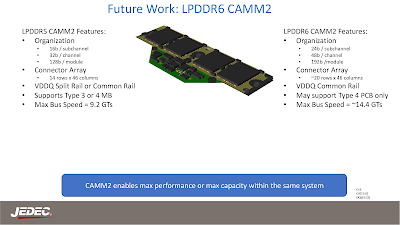
LPDDR6 promises to revolutionize iGPU performance. With a single CAMM2 LPDDR6 module offering a 192-bit bus, theoretical bandwidth can reach approximately 322 GB/s:
- Bits to bytes conversion: 192 bits / 8 bits/byte = 24 bytes
- Transfer rate calculation: 14,400,000,000 transfers/second * 24 bytes/transfer = 345,600,000,000 bytes/second
- Conversion to gigabytes per second: 345,600,000,000 bytes/second / 1,073,741,824 bytes/GB ≈ 322 GB/s
This represents a 2.5x improvement in theoretical bandwidth, potentially enabling iGPUs in mainstream notebooks and handhelds to rival popular dGPUs like the NVIDIA GeForce RTX 4060 or AMD Radeon RX 7600XT. The technology behind it;
The JEDEC JC-45 Committee is actively developing two groundbreaking memory module technologies: a new Tall MRDIMM form factor and a next-generation CAMM module for LPDDR6.
The Tall MRDIMM aims to significantly increase memory bandwidth and capacity by allowing for twice the number of DRAM single-die packages on the module without requiring 3D stacking. This innovative approach leverages a taller form factor while maintaining the existing DRAM package.
Complementing this, JC-45 is developing a cutting-edge CAMM module specifically designed for LPDDR6 operation at speeds exceeding 14.4 GT/s. This advanced module will feature a 24-bit subchannel, a 48-bit channel, and a connector array.
Both these projects are crucial for advancing memory technology and are currently under development within the JC-45 Committee. JEDEC strongly encourages industry participation to shape the future of memory standards. Membership provides valuable benefits, including access to pre-publication proposals and early insights into critical projects like MRDIMM and the next-generation CAMM.
Source: JEDEC Unveils Plans


Nenhum comentário:
Postar um comentário